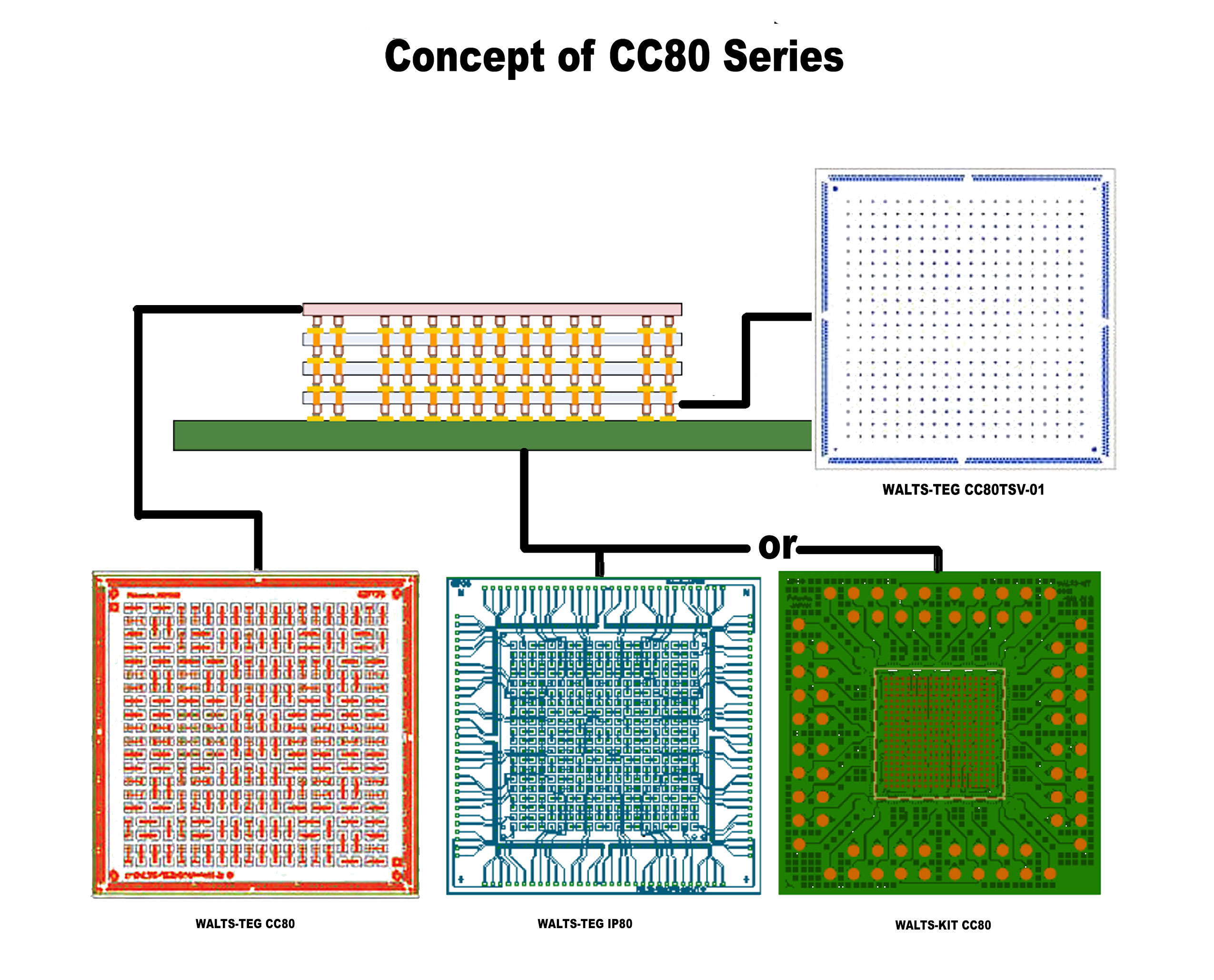
Chip Structure
- Base Layer : P-TEOS*
- Metal Layer : TiN / AI-0.5%Cu
- Passivation Layer : HDP* / P-SiN (option) Polymide
*TEOS : Tetraethoxysilane
*HDP : High Density Plasma
| Specifications | |
| Wafer Size | 8 inch |
| Wafer Thickness | 725±25μm |
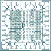
| Chip Size | 10.0mm |
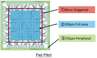
| Pad pitch | 80μm Staggered (Inner pad) 300μm Full area (Center core) 250μm Peripheral (Outer pad) |
| Function | Daisy Chain |
| Pad config | Peripheral and Full Area |
| Pad Size | 58 μm 58 μm 110 μm |
| Passivation opening | 48 μm 48 μm 100 μm |
| Scribe width | 100μm |
| Number of Pad | 648 400 124 |
| Number of Chip | 228 chips/wafer |
| Surface Spec of Electrode | Electroless Ni/Au plating, Al-Si(0.5%) |